- CR Home
- CR Group
- 中文版


 Structure of Panel Packaging Products

 Panel and Products of SIPLP Microelectronic

 Advantages of SIPLP’s Advanced Packaging Technology
●Bumping/Copper Pillar middle process is not needed.
●Thick Trace can support bigger current.
●Able to realize 6-side protection and the reliability reaches MSL1. Especially suitable for automobile electronics.
●Thinner than FC (no substrate or lead frame)
●No Bumping, unnecessary Reflow, seamless connection, better product performance and higher reliability.
●Smaller parasitic effect
●Smaller on-resistance RDSon
●Flexible technology. Especially suitable for MCM multiple chips packaging and power module packaging
●Able to make Copper Clip PQFN and can realize double cooling.
●Especially suitable for embedded passive device of power package, multiple chips package and module package.
●EMI shielding Anti-electromagnetic interference
●One Panel one Lot
●More suitable for the packaging of the third-generation semiconductors such as SiC and GaN.

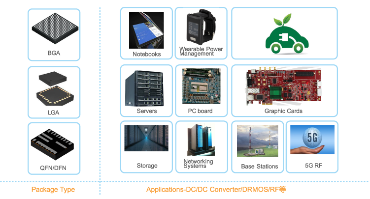
 SiPLP Packaging Way and Main Application Fields